Phase transitions between metastable states can provide stark contrasts in electronic and optical properties that are useful for many applications. “Conventional” PCMs, such as Ge-Sb-Te alloys, exhibit remarkable properties: they can be amorphized and crystallized in picoseconds, yet can remain stable against spontaneous changes of state for many years. They show large contrast in electrical conductivity and refractive index between phases, which have led to their applications in electrical PCRAM and optical DVDs. The origin of these useful properties has been the subject of intense research. Recent studies suggest that the crystalline phases of PCMs are extraordinary due to their bonding network and large concentration of vacancies; both dynamically evolve under electrical and optical stimuli, producing distortions that trigger the collapse of long-range order and generate amorphous phases. Furthermore, research has shown that assembling point defects into planar defects can lower the power required to switch between states, thereby highlighting the opportunity for engineering defects to optimize PCMs.
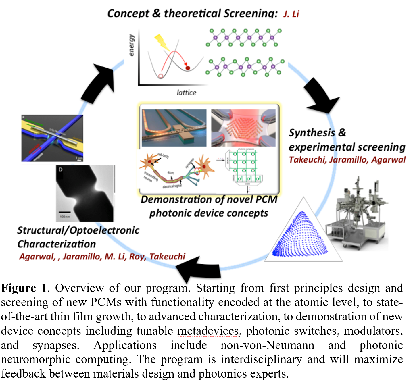
Tremendous opportunities exist if we can better understand and control the mechanisms behind phase change and optoelectronic contrast in existing PCMs. To-date, the lack of a coherent approach has hindered the discovery of new PCMs. Our team addresses this challenge by programming the desired functionality at the atomic level. We propose a holistic approach ranging from first-principles design and computational screening of new PCMs enabled by defects and polymorphism, to state-of-the-art synthesis, to advanced characterization including in situ microscopy, and finally to demonstrations of novel photonic devices and systems.
Thrust 1: Encoding functionality at the atomic level with in-silico design of phase change materials.
PCMs have been mostly discovered through serendipity, starting with the observation of an abrupt change in a bulk property (e.g. conductivity, refractive index or color). The associated thermodynamics and kinetics are then studied, and applications proposed. The atomic-scale origins of the phase change and contrasting properties are eventually agreed upon, and then researchers can formulate materials design principles. The history of the GeTe-Sb2Te3 system (GST) exemplifies this process1.
We will accelerate the discovery of PCMs and expand their applications by reversing the traditional path to discovery. Instead of taking for granted bulk phase transitions as found in nature, we will start with atomic-scale phenomena that are known to support useful phase-change properties, and use theory to design candidate materials. We will use thin film deposition and defect-engineering techniques to synthesize selected materials, and an elaborate characterization program to catalog optoelectronic properties and verify their microscopic mechanisms. These materials will then be integrated with device platforms to study their feasibility for new photonics applications. Our work will be guided by two themes: utilizing polymorphism along with point defect engineering to design the next generation of PCMs with precisely controlled properties.
Thrust 2: PCM-based Photonics.
Integrated photonics promises to revolutionize computing by eliminating the von-Neumann bottleneck associated with shuttling information between CPU and memory, thereby overcoming the bandwidth and power limitations of conventional electronics. In photonic systems, active components such as modulators, routers, and switches are needed to control light. To compete with all-electronic systems, active optical components need to consume energy at <1 fJ/bit, which is challenging with conventional materials. PCMs are promising because, unlike optoelectronic effects in conventional materials (e.g. Si, LiNbO3), the properties of PCMs can change rapidly and drastically, and can be maintained in non-volatile states without sustained electrical or optical bias. Therefore, photonic devices utilizing PCMs can feature smaller dimensions and lower power consumption than devices based on traditional optoelectronic materials. Furthermore, the discovery of new PCMs (Thrust 1) based on polymorphism and defect engineering can lead to the development of device concepts based on new functionalities such as optoelectronic chemical sensing, optically switched magnetism, and re-writable optoelectronic circuits.

PCM-based photonic neuromorphic computing.
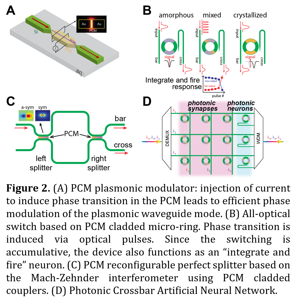
Optical neuromorphic computing can utilize the unparalleled bandwidth afforded by photonics to overcome the limitations of all-electronic artificial neural networks (ANN). By incorporating new functionalities in PCMs, we will enable applications that mimic our brain in image recognition and distributed sensing. Photonic PCMs proposed here will be suitable for cross-bar analog memory arrays that can implement neuromorphic computation patterns with high efficacy and no cross-talk. The multi-level, non-volatile operation of PCM photonic devices makes them suitable for synaptic elements simulating the “integrate and fire” properties of neurons (Fig. 2B). In this thrust, we will address the challenges to assembling a prototypical photonic ANN architecture, which will be fast and efficient. We will explore the mapping advantages of large and fast photonic crossbars for ANNs, and evaluate the energy and time requirements for their synaptic read/write operations compared to conventional electronic crossbars. We will also investigate the usage of photonic devices for spiking neurons. Interfacing photonic crossbars with CMOS neurons and efficient learning in a neural network requires interfacing circuitry to support homeostasis and synaptic decay. We will demonstrate an efficient approach to interfacing required for on-chip neuromorphic learning.