2024

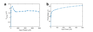
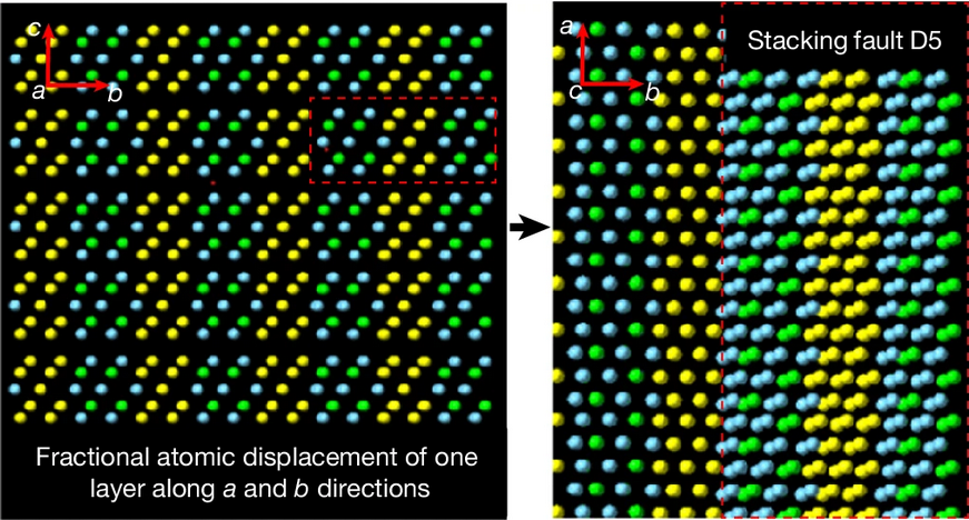
116. Gaurav Modi, Shubham K. Parate, Chaoh Kwon, Andrew C. Meng, Utkarsh Khandelwal, Anudeep Tullibilli, James Horwath, Peter K. Davies, Eric A. Stach, Ju Li, Pavan Nukala and Ritesh Agarwal “Electrically driven long-range solid-state amorphization in ferroic In2Se3.”; Nature [Link].

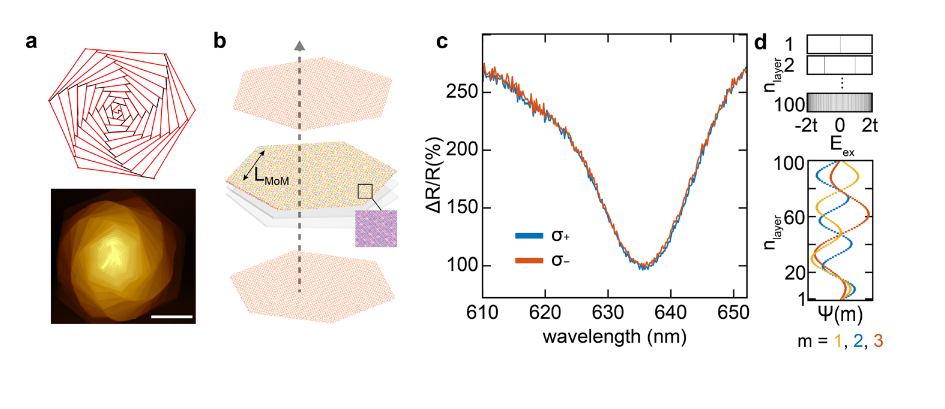
116. Zhurun Ji , Yuzhou Zhao , Yicong Chen , Ziyan Zhu , Yuhui Wang, Wenjing Liu , Gaurav Modi 1 , Eugene J. Mele , Song Jin and Ritesh Agarwal “Opto-twistronic Hall effect in a three-dimensional spiral lattice.”; Nature [Link]; arXiv [Link]

Click to enlarge
Click to enlarge

115. Utkarsh Khandelwal, Harshvardhan Jog, Shupeng Xu, Yicong Chen, Kejian Qu, Chengxi Zhao, Eugene Mele, Daniel P. Shoemaker, and Ritesh Agarwal “Strong Chirality Suppression in 1-D correlated Weyl Semimetal” (TaSe4)2I”; arXiv[Link]

Click to enlarge

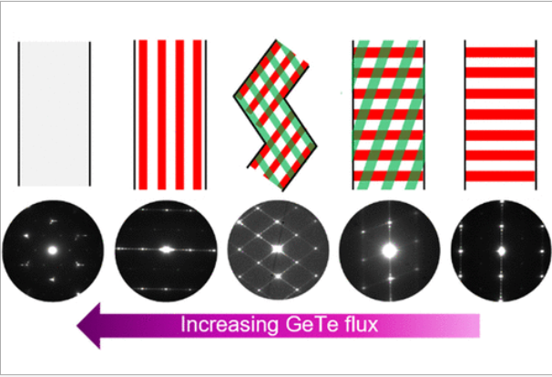
114. Gaurav Modi, Andrew C. Meng, Srinivasan Rajagopalan, Rangarajan Thiruvengadam, Peter K. Davies, Eric A. Stach, and Ritesh Agarwal “Controlled Self-Assembly of Nanoscale Superstructures in Phase-Change Ge–Sb–Te Nanowires”; Nano Lett [Link]

Click to enlarge

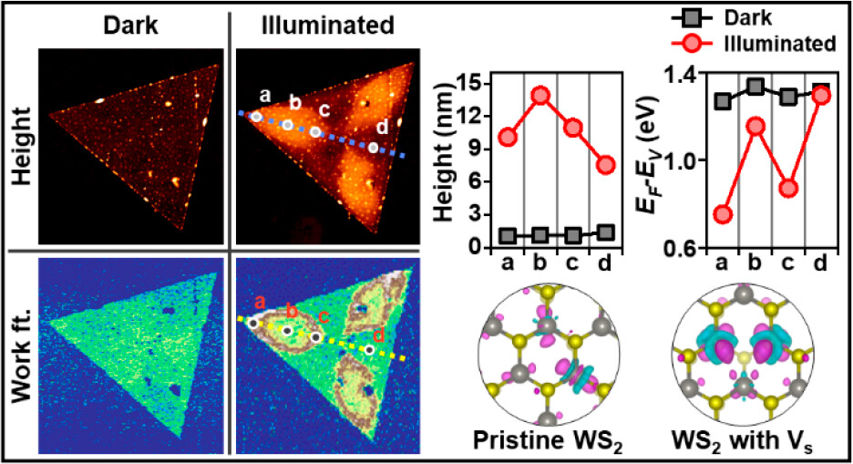
113. Young-Chul Leem, Zhenyao Fang, Yun-Kyung Lee, Na-Yeong Kim, Arvin Kakekhani, Wenjing Liu, Sung-Pyo Cho, Cheolsu Kim, Yuhui Wang, Zhurun Ji, Abhirup Patra, Leeor Kronik, Andrew M. Rappe, Sang-Youp Yim, and Ritesh Agarwal “Optically Triggered Emergent Mesostructures in Monolayer WS2“; Nano Lett [Link]

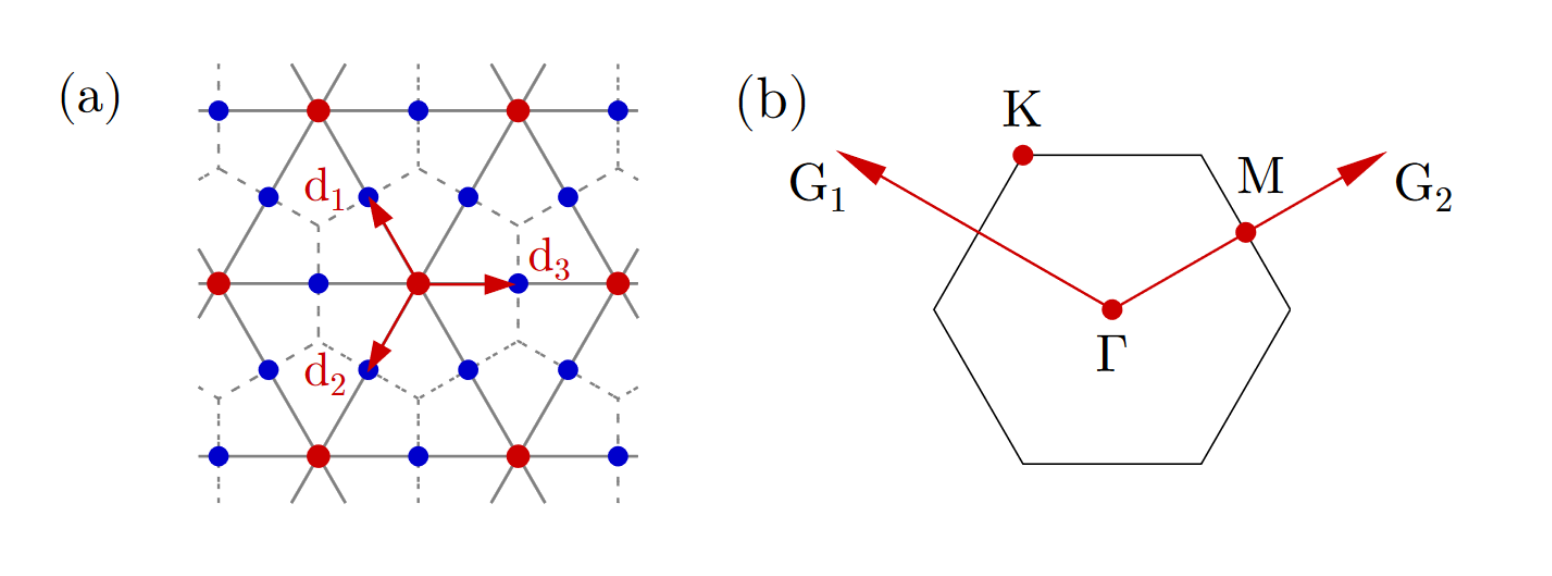
112. Yuhui Wang, Shupeng Xu, Liang Feng, Ritesh Agarwal “Simple realization of a fragile topological lattice with quasi flat-bands in a microcavity array”; Physical Review B [Link], arXiv [Link]

Click to enlarge
Click to enlarge

HOLOGRAPHIC MESSAGES: SCI-FI STAPLE EDGES CLOSER TO REALITY WITH MULTI-LAYERED HOLOGRAMS

BY HANNAH OSBORNE ON 5/10/17 AT 9:01 AM

Holographic messages, a regular feature in science fiction, could be moving closer to reality. Researchers have created holograms that change from one image to another—a breakthrough that could one day lead to the development of animated holograms, and maybe even Star Wars-style messages.

Scientists led by Ritesh Agarwal, from the University of Pennsylvania, were building on previous research where they used gold nanorods embedded into a stretchable film to create 3D and multicolored holograms. In their latest study, published in Nano Letters, the team worked out how they could stretch a metasurface film (a flat, ultra-thin, nanostructured surface) to get the holographic image to change into something different.

There is great scientific interest in the development of holographic messages. Being able to transmit 3D images from one location to another in real-time has far-reaching applications, including in medicine—during surgery, for example—manufacturing and entertainment.

But it also has security implications, as hologram messages would be more difficult to intercept. In an email interview with Newsweek, Agarwal and study co-author Stephanie Malek explain: “Holograms allow signals to be sent via a secure channel, while transmission of photographs can be intercepted. For the other side to read out the hologram, they need to know what type of light source needs to be used.”

They said that while photographs encode information based on the amplitude of light alone, holograms use both amplitude and phase, the latter of which is responsible for the modulation of a wave in time and space. “Holograms also use this phase information to store data, which allows more to be stored and transmitted in a safe manner,” they add.

In their study, which is currently a proof of the concept, the team looked at how a holographic image changed when they stretched the material generating it. They also looked at how far the image plane would move from its original position. They then used computer models and experiments to make calculations in order to create a multi-layered hologram made up of two to three images.

The hologram they created could be stretched so one image would be change into another as the material was changed. Agarwal and Malek say the biggest challenge was creating the stretchable material: “We had to make sure that the repeated process of stretching and releasing the polymer does not dislodge the precise alignment and placement of nanorods in the polymer. Also, the designs needed to ensure minimum interference between different images.”

The next big step in this research will be to create multicolor stretchable holograms: “Then we are working to encode many more images in the metasurface hologram to eventually make some sort of animation,” Agarwal and Malek say. “Finally, the holy grail of this area would be to also obtain a tunable response by applying varying voltage to the device, making [the holograms] more compatible with all kinds of applications, including virtual reality.” Tunability refers to the ability to tune the metasurface to different wavelengths so it can be used for different purposes.

“Future applications might involve metasurface holograms that transmit multiple secret messages that are accessible by stretching or applying voltage, or hologram images that are also animated upon applying some sort of stimuli (mechanical or chemical force, applied fields etc). These concepts can then be easily extended to other applications related to virtual reality and optical and secure communication. Right now VR devices are very bulky and thick, but if tunability can be programmed as we have shown (and still working on it to extend and improve), then the same VR experience can be obtained by wearing “regular” glasses.”

Asked whether sci-fi hologram messages become a reality, they say: “We had not necessarily considered developing talking holograms like the ones in Star Wars but that may be possible by also encoding audio information via some other means.”
PROPOSAL WHITE PAPER

Multidisciplinary University Research Initiative (MURI)

Office of Naval Research (ONR)
Topic 11 (ONR): Phase Change Materials for Photonics

Estimated Cost:
$1,500,000 per year for five years.

Proposer’s technical point of contact:

Prof. Ritesh Agarwal

Department of Material Science and Engineering
University of Pennsylvania
E-mail: riteshag@seas.upenn.edu
Tel: 215-573-3037
FAX: 215-573-2128

Research Topic Chief:

Dr. Brian R. Bennett, ONR/312
E-mail: brian.r.bennett@navy.mil
Dr. Antti J. Makinen, ONR/332
E-mail: antti.makinen@navy.mil

Professor

Prof. Ritesh Agarwal
MSE, University of Pennsylvania

[Group Webpage]


Prof. Rafael Jaramillo
MSE, MIT

[Group Webpage]


Prof. Ju Li
MSE, MIT

[Group Webpage]


Prof. Mo Li
ECE, University of Minnesota

[Group Webpage]


Prof. Kaushik Roy
ECE, Purdue University

[Group Webpage]


Prof. Ichiro Takeuchi
MSE, University of Maryland

[Group Webpage]

Spatially dispersive circular photogalvanic effect in a Weyl semimetal

Step forward for computing by light

From BBC news:

Engineers and physicists have discovered a property of silicon which could aid the development of faster computers.

Currently, copper wires transfer information in a computer; the process is slowed down as the wires heat up.

“Photonic” and “spintronic” computing is the principle of transferring information by light or electron spin.

This new property means that silicon-based light detectors identify spin, so more information can be transferred.

Spin is a property of sub-atomic particles, which influences the ordering of electrons and nuclei in atoms and molecules.

The discovered property is usually observed in materials containing heavy elements, which are difficult to integrate into existing computing systems that are composed mainly of silicon.

Silicon is a highly symmetrical crystal, but by changing the geometry of it, the team was able to impart “chiral” properties to it. Something is chiral if the mirror image of the object cannot be superimposed on the original.
This chirality means that silicon-based detectors are able to detect the spin of electrons and light, and as a result allow more information to be transmitted.

“The whole computer running with light is a distant dream, but some copper interconnectors can be replaced with light and photo-detector devices,” Professor Ritesh Agarwal, who led this study at the University of Pennsylvania, told BBC News.

“This is only around five years away from now. The technology already exists, but this can bring added functionality.”

The discovery was made by accident, while investigating heavier materials.

As well as discovering chirality in silicon, this study has wider implications for materials science.

“It’s the same silicon, all we’ve done is cut it in a particular direction,” explained Professor Ritesh Agarwal.

This is a step towards engineering new, useful properties by changing the geometry of a material.

(No title)


Mariam Georges (joint with Dan Gianola, MSE), expected May 2011.

Christopher Rodd


Nanowire-Conducting Polymer Hybrid Systems

May 2011

Brian Piccione


Light-Matter Coupling in Nanowire Optical Cavities

http://www.seas.upenn.edu/~bpic/

Carlos Aspetti


Nanowire plasmonics

May 2014

Pavan Nukala


Phase Change Nanowires: insitu microscopy analysis

May 2014

http://www.seas.upenn.edu/~pnukala/

Rahul Agarwal


Chalcogenide nanowires, Phase change and thermoelectrics

May 2015

Joohee Park


Nanowire Optics

May 2015

Siddharth Ghosh


(Jointly with G. Piazza, ESE, Penn)

Nanowire Optomechanics

May 2014

(No title)


Haofeng Li (Nanowire Photovoltaics), expected May 2011

Hello world!

Welcome to WordPress. This is your first post. Edit or delete it, then start blogging!