AUTUM C. PYLANT, NEWS EDITOR, AUTUM.PYLANT@PHOTONICS.COM
PHILADEPHIA, Oct. 1, 2018 —
AUTUM C. PYLANT, NEWS EDITOR, AUTUM.PYLANT@PHOTONICS.COM
PHILADEPHIA, Oct. 1, 2018 —
BY HANNAH OSBORNE ON 5/10/17 AT 9:01 AM
Holographic messages, a regular feature in science fiction, could be moving closer to reality. Researchers have created holograms that change from one image to another—a breakthrough that could one day lead to the development of animated holograms, and maybe even Star Wars-style messages.
Scientists led by Ritesh Agarwal, from the University of Pennsylvania, were building on previous research where they used gold nanorods embedded into a stretchable film to create 3D and multicolored holograms. In their latest study, published in Nano Letters, the team worked out how they could stretch a metasurface film (a flat, ultra-thin, nanostructured surface) to get the holographic image to change into something different.
There is great scientific interest in the development of holographic messages. Being able to transmit 3D images from one location to another in real-time has far-reaching applications, including in medicine—during surgery, for example—manufacturing and entertainment.
But it also has security implications, as hologram messages would be more difficult to intercept. In an email interview with Newsweek, Agarwal and study co-author Stephanie Malek explain: “Holograms allow signals to be sent via a secure channel, while transmission of photographs can be intercepted. For the other side to read out the hologram, they need to know what type of light source needs to be used.”
They said that while photographs encode information based on the amplitude of light alone, holograms use both amplitude and phase, the latter of which is responsible for the modulation of a wave in time and space. “Holograms also use this phase information to store data, which allows more to be stored and transmitted in a safe manner,” they add.
In their study, which is currently a proof of the concept, the team looked at how a holographic image changed when they stretched the material generating it. They also looked at how far the image plane would move from its original position. They then used computer models and experiments to make calculations in order to create a multi-layered hologram made up of two to three images.
The hologram they created could be stretched so one image would be change into another as the material was changed. Agarwal and Malek say the biggest challenge was creating the stretchable material: “We had to make sure that the repeated process of stretching and releasing the polymer does not dislodge the precise alignment and placement of nanorods in the polymer. Also, the designs needed to ensure minimum interference between different images.”
The next big step in this research will be to create multicolor stretchable holograms: “Then we are working to encode many more images in the metasurface hologram to eventually make some sort of animation,” Agarwal and Malek say. “Finally, the holy grail of this area would be to also obtain a tunable response by applying varying voltage to the device, making [the holograms] more compatible with all kinds of applications, including virtual reality.” Tunability refers to the ability to tune the metasurface to different wavelengths so it can be used for different purposes.
“Future applications might involve metasurface holograms that transmit multiple secret messages that are accessible by stretching or applying voltage, or hologram images that are also animated upon applying some sort of stimuli (mechanical or chemical force, applied fields etc). These concepts can then be easily extended to other applications related to virtual reality and optical and secure communication. Right now VR devices are very bulky and thick, but if tunability can be programmed as we have shown (and still working on it to extend and improve), then the same VR experience can be obtained by wearing “regular” glasses.”
Asked whether sci-fi hologram messages become a reality, they say: “We had not necessarily considered developing talking holograms like the ones in Star Wars but that may be possible by also encoding audio information via some other means.”
Project Managers:
Dr. Brian R. Bennett, ONR
Dr. Antti J. Makinen, ONR
Multidisciplinary University Research Initiative (MURI)
Office of Naval Research (ONR)
Topic 11 (ONR): Phase Change Materials for Photonics
Estimated Cost:
$1,500,000 per year for five years.
Proposer’s technical point of contact:
Prof. Ritesh Agarwal
Department of Material Science and Engineering
University of Pennsylvania
E-mail: riteshag@seas.upenn.edu
Tel: 215-573-3037
FAX: 215-573-2128
Research Topic Chief:
Dr. Brian R. Bennett, ONR/312
E-mail: brian.r.bennett@navy.mil
Dr. Antti J. Makinen, ONR/332
E-mail: antti.makinen@navy.mil
Professor

Prof. Ritesh Agarwal
MSE, University of Pennsylvania
[Group Webpage]

Prof. Rafael Jaramillo
MSE, MIT
[Group Webpage]

Prof. Ju Li
MSE, MIT
[Group Webpage]

Prof. Mo Li
ECE, University of Minnesota
[Group Webpage]

Prof. Kaushik Roy
ECE, Purdue University
[Group Webpage]

Prof. Ichiro Takeuchi
MSE, University of Maryland
[Group Webpage]

Phase transitions between metastable states can provide stark contrasts in electronic and optical properties that are useful for many applications. “Conventional” PCMs, such as Ge-Sb-Te alloys, exhibit remarkable properties: they can be amorphized and crystallized in picoseconds, yet can remain stable against spontaneous changes of state for many years. They show large contrast in electrical conductivity and refractive index between phases, which have led to their applications in electrical PCRAM and optical DVDs. The origin of these useful properties has been the subject of intense research. Recent studies suggest that the crystalline phases of PCMs are extraordinary due to their bonding network and large concentration of vacancies; both dynamically evolve under electrical and optical stimuli, producing distortions that trigger the collapse of long-range order and generate amorphous phases. Furthermore, research has shown that assembling point defects into planar defects can lower the power required to switch between states, thereby highlighting the opportunity for engineering defects to optimize PCMs.
Tremendous opportunities exist if we can better understand and control the mechanisms behind phase change and optoelectronic contrast in existing PCMs. To-date, the lack of a coherent approach has hindered the discovery of new PCMs. Our team addresses this challenge by programming the desired functionality at the atomic level. We propose a holistic approach ranging from first-principles design and computational screening of new PCMs enabled by defects and polymorphism, to state-of-the-art synthesis, to advanced characterization including in situ microscopy, and finally to demonstrations of novel photonic devices and systems.
Broad Research Thrusts
Thrust 1: Encoding functionality at the atomic level with in-silico design of phase change materials.
PCMs have been mostly discovered through serendipity, starting with the observation of an abrupt change in a bulk property (e.g. conductivity, refractive index or color). The associated thermodynamics and kinetics are then studied, and applications proposed. The atomic-scale origins of the phase change and contrasting properties are eventually agreed upon, and then researchers can formulate materials design principles. The history of the GeTe-Sb2Te3 system (GST) exemplifies this process1.
We will accelerate the discovery of PCMs and expand their applications by reversing the traditional path to discovery. Instead of taking for granted bulk phase transitions as found in nature, we will start with atomic-scale phenomena that are known to support useful phase-change properties, and use theory to design candidate materials. We will use thin film deposition and defect-engineering techniques to synthesize selected materials, and an elaborate characterization program to catalog optoelectronic properties and verify their microscopic mechanisms. These materials will then be integrated with device platforms to study their feasibility for new photonics applications. Our work will be guided by two themes: utilizing polymorphism along with point defect engineering to design the next generation of PCMs with precisely controlled properties.
Thrust 2: PCM-based Photonics.
Integrated photonics promises to revolutionize computing by eliminating the von-Neumann bottleneck associated with shuttling information between CPU and memory, thereby overcoming the bandwidth and power limitations of conventional electronics. In photonic systems, active components such as modulators, routers, and switches are needed to control light. To compete with all-electronic systems, active optical components need to consume energy at <1 fJ/bit, which is challenging with conventional materials. PCMs are promising because, unlike optoelectronic effects in conventional materials (e.g. Si, LiNbO3), the properties of PCMs can change rapidly and drastically, and can be maintained in non-volatile states without sustained electrical or optical bias. Therefore, photonic devices utilizing PCMs can feature smaller dimensions and lower power consumption than devices based on traditional optoelectronic materials. Furthermore, the discovery of new PCMs (Thrust 1) based on polymorphism and defect engineering can lead to the development of device concepts based on new functionalities such as optoelectronic chemical sensing, optically switched magnetism, and re-writable optoelectronic circuits.

PCM-based photonic neuromorphic computing.
Optical neuromorphic computing can utilize the unparalleled bandwidth afforded by photonics to overcome the limitations of all-electronic artificial neural networks (ANN). By incorporating new functionalities in PCMs, we will enable applications that mimic our brain in image recognition and distributed sensing. Photonic PCMs proposed here will be suitable for cross-bar analog memory arrays that can implement neuromorphic computation patterns with high efficacy and no cross-talk. The multi-level, non-volatile operation of PCM photonic devices makes them suitable for synaptic elements simulating the “integrate and fire” properties of neurons (Fig. 2B). In this thrust, we will address the challenges to assembling a prototypical photonic ANN architecture, which will be fast and efficient. We will explore the mapping advantages of large and fast photonic crossbars for ANNs, and evaluate the energy and time requirements for their synaptic read/write operations compared to conventional electronic crossbars. We will also investigate the usage of photonic devices for spiking neurons. Interfacing photonic crossbars with CMOS neurons and efficient learning in a neural network requires interfacing circuitry to support homeostasis and synaptic decay. We will demonstrate an efficient approach to interfacing required for on-chip neuromorphic learning.
 Click to enlarge
82.
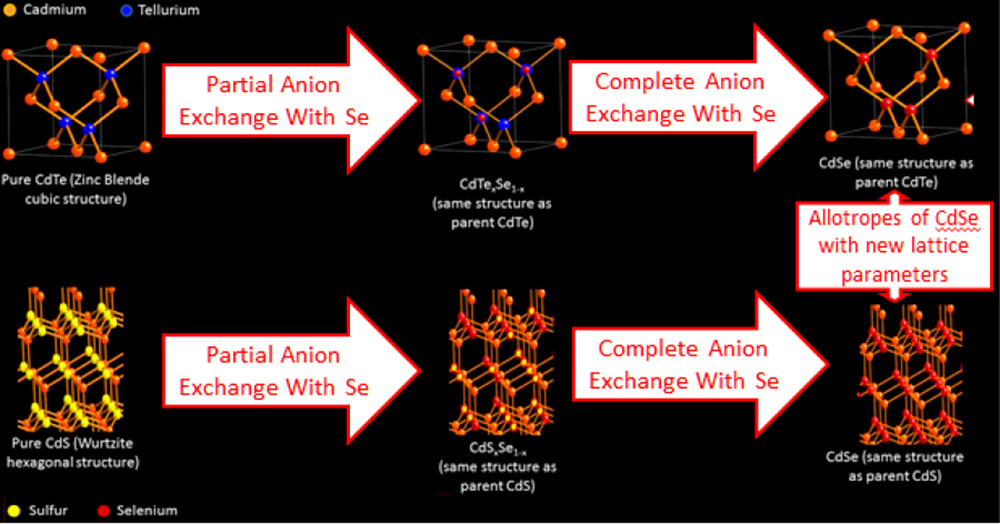
Rahul Agarwal, Nadia M Krook, Ming-Liang Ren, Liang Z Tan, Wenjing Liu, Andrew M Rappe, Ritesh Agarwal, “Anion exchange in II–VI semiconducting nanostructures via atomic templating”, Nano Letters. [Link]
 Click to enlarge
81.
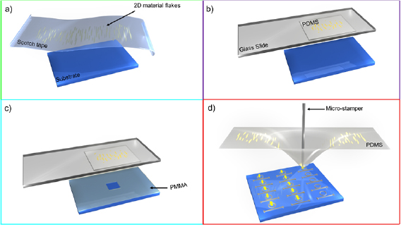
Rohit A Hemnani, Jason P Tischler, Caitlin Carfano, Rishi Maiti, Mohammad H Tahersima, Ludwig Bartels, Ritesh Agarwal, Volker J Sorger, “2D material printer: a deterministic cross contamination-free transfer method for atomically layered materials”, 2D Materials. [Link]
 Click to enlarge
80.
Vo Tien Phong, Zachariah Addison, Seongjin Ahn, Hongki Min, Ritesh Agarwal, E. J. Mele, “Optically-Controlled Orbitronics on a Triangular Lattice”, Arxiv. [Link]
 Click to enlarge
79.
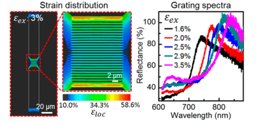
Wenxiang Chen, Wenjing Liu, Yijie Jiang, Mingliang Zhang, Naixin Song, Nicholas J. Greybush, Jiacen Guo, Anna K. Estep, Kevin T. Turner, Ritesh Agarwal, and Cherie R. Kagan, “Ultrasensitive, Mechanically Responsive Optical Metasurfaces via Strain Amplification”, ACS Nano. [Link]
 Click to enlarge
78.
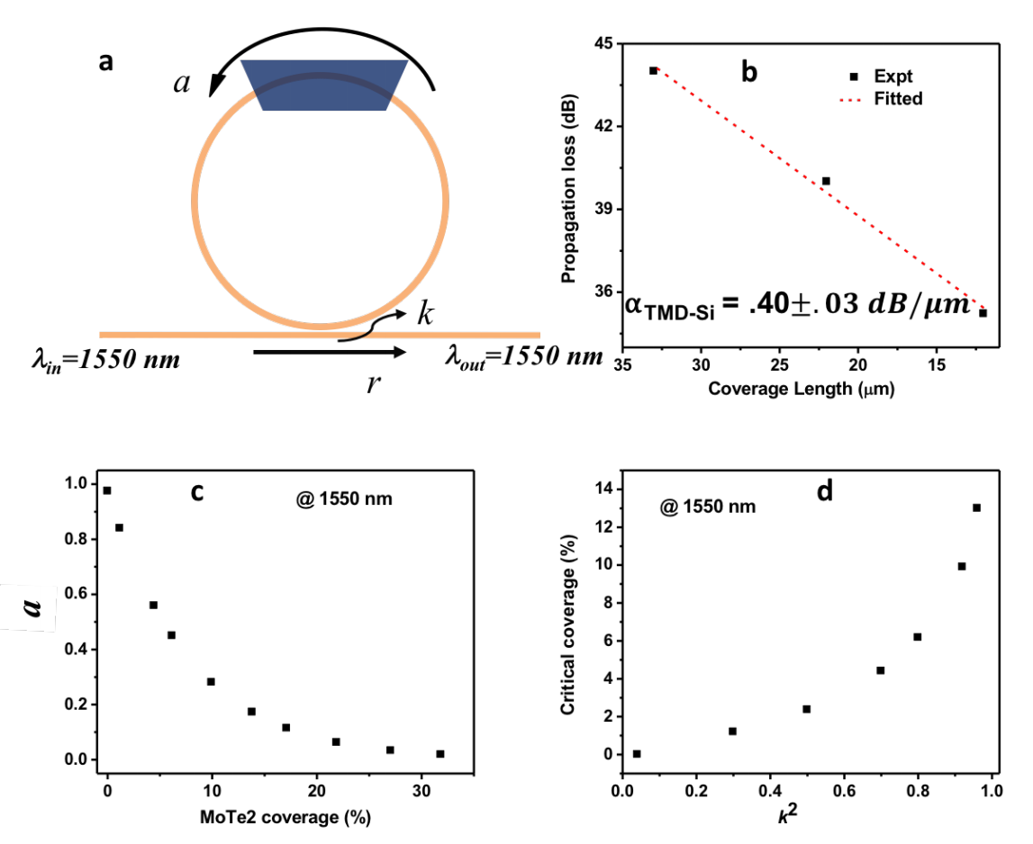
Rishi Maiti, Rohit Hemnani, Rubab Amin, Zhizhen Ma, Mohammad Tahersima, Thomas A. Empante, Hamed Dalir, Ritesh Agarwal, Ludwig Bartels, Volker J. Sorger, “Microring Resonators Coupling Tunability by Heterogeneous 2D Material Integration”, Arxiv. [Link]
 Click to enlarge
77.
Ming-Liang Ren, Jacob S. Berger, Wenjing Liu, Gerui Liu & Ritesh Agarwal, “Strong modulation of second-harmonic generation with very large contrast in semiconducting CdS via high-field domain”,Nature Communications. [Link]
 Click to enlarge
76.
Zhizhen Ma, Rohit Hemnani, Ludwig Bartels, Ritesh Agarwal, Volker J. Sorger, “2D materials in electro-optic modulation: energy efficiency, electrostatics, mode overlap, material transfer and integration”,Applied Physics A. [Link]