Tailoring hot-exciton emission and lifetimes in semiconducting nanowires via whispering-gallery nanocavity plasmons
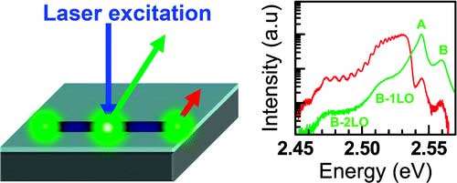
One-dimensional polaritons with size-tunable and enhanced coupling strengths in semiconductor nanowires
Hee-Suk Chung completes his post-doctoral candidature
Hee-Suk Chung has completed his post-doctoral candidature with the group. He is headed to Samsung, South Korea. The group wishes him all the very best for his future and will surely miss him and his expertise!
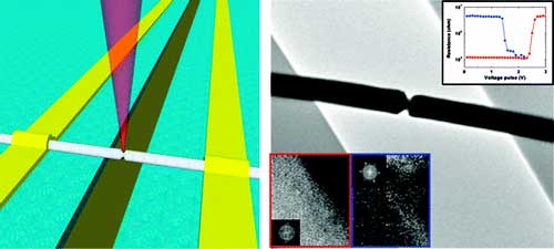
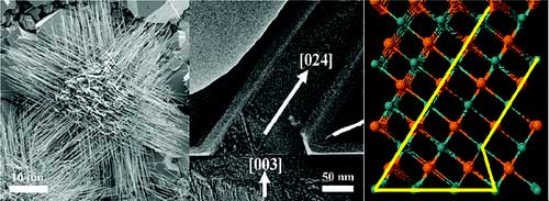
High Resolution Transmission Electron Microscopy Study of Electrically-Driven Phase Change Phenomena in Ge2Sb2Te5 Nanowires
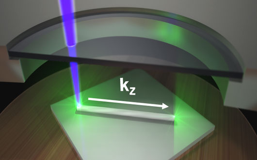
Incorporating Polaritonic Effects in Semiconductor Nanowire Waveguide Dispersion
Nanowire Transformation by Size-Dependent Cation Exchange Reactions
2011
 Click to enlarge
39.
J. D. Cox, M. R. Singh, C. Racknor, and R. Agarwal, “Switching in Polaritonic–Photonic Crystal Nanofibers Doped with Quantum Dots”, Nano Letters. [Link]
 Click to enlarge
38.
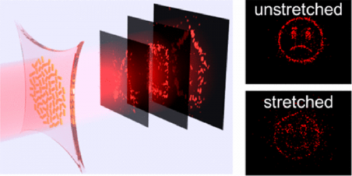
Christopher M. Rodd and Ritesh Agarwal, “Enhancement of Interfacial Polymer Crystallinity Using Chromism in Single Inorganic Nanowire–Polymer Nanohybrids for Photovoltaic Applications”, Nano Letters. [Link]
 Click to enlarge
37.
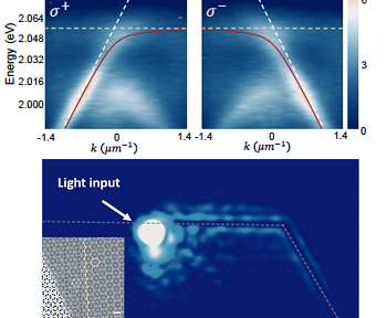
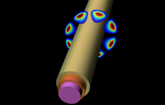
Chang-Hee Cho, Carlos O. Aspetti, Michael E. Turk, James M. Kikkawa, Sung-Wook Nam & Ritesh Agarwal, “Tailoring hot-exciton emission and lifetimes in semiconducting nanowires via whispering-gallery nanocavity plasmons”, Nature Materials. [Link]
 Click to enlarge
36.
Lambert K. van Vugt, Brian Piccione, Chang-Hee Cho, Pavan Nukala, and Ritesh Agarwal, “One-dimensional polaritons with size-tunable and enhanced coupling strengths in semiconductor nanowires”, PNAS. [Link]
 Click to enlarge
35.
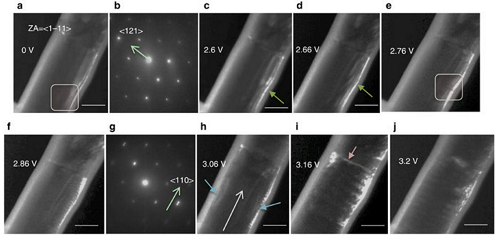
Y. Jung, S.W. Nam, and R. Agarwal, “High Resolution Transmission Electron Microscopy Study of Electrically-Driven Phase Change Phenomena in Ge2Sb2Te5 Nanowires”.Nano Letters[Link]
 Click to enlarge
34.
Y. Jung, R. Agarwal, C.Y. Yang and R. Agarwal*, "Chalcogenide Phase-change Memory Nanotubes for Lower Writing Current Operation", Nanotechnology, invited paper for the nanoscale memory issue. [Link].
 Click to enlarge
33.
L. K. Van Vugt, B. Piccione, C.H. Cho, C. Aspetti, A. Wirshbha and R. Agarwal, “Variable Temperature Spectroscopy of as-grown and Passivated CdS Nanowire Optical Waveguide Cavities”, J. Physical. Chemistry, invited paper for special issue for G. R. Fleming. [Link]
2010
 Click to enlarge
32.
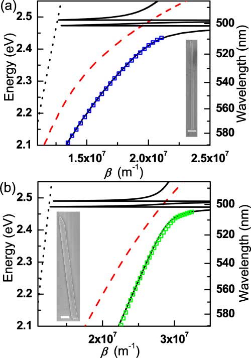
L.K. Van Vugt, B. Piccione, and R. Agarwal*, “Incorporating Polaritonic Effects in Semiconductor Nanowire Waveguide Dispersion”, Applied Physics Letters [Link]
 Click to enlarge
31.
M. Mitra, Y. Jung, and R. Agarwal, “Extremely Low Drift of Resistance and Threshold Voltage in Amorphous Phase Change Nanowire Devices”, Applied Physics Letters[Link]
 Click to enlarge
30.
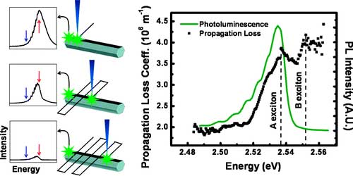
B. Piccione, L. K. Van Vugt and R. Agarwal, “Propagation Loss Spectroscopy on Single Nanowire Active Waveguides”, Nano Letters [Link]
 Click to enlarge
29.
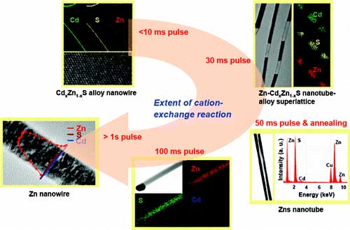
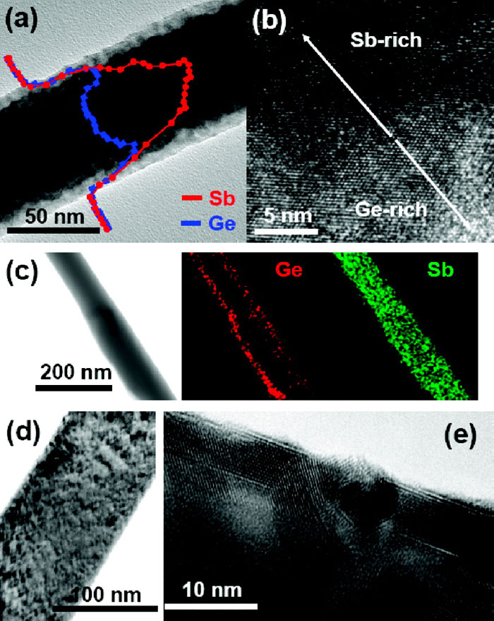
B. Zhang, Y. Jung, H.-S. Chung, L. K. Van Vugt and R. Agarwal’ “Nanowire Transformation by Size-Dependent Cation Exchange Reactions”, Nano Letters [Link]
2009
 Click to enlarge
28.
H.-S. Chung, Y. Jung, S. C. Kim, D. H. Kim, K. H. Oh and R. Agarwal, “Epitaxial Growth and Ordering of GeTe Nanowires on Microcrystals Determined by Surface Energy Minimization”, Nano Letters[Link]
 Click to enlarge
27.
Y. Jung, C.-Y. Yang, S.-H. Lee and R. Agarwal, Phase-Change Ge-Sb Nanowires: Synthesis, “Memory Switching, and Phase-Instability”,Nano Letters[Link]
 Click to enlarge
26.
A.T. Jennings, Y. Jung, J. Engel, and R. Agarwal. "Diameter-Controlled Synthesis of Phase-Change GeTe Nanowires,"J. Phys. Chem. C[Link]
 Click to enlarge
25.
L.K. van Vugt, B. Zhang, B. Piccione, A. Spector and R. Agarwal, “Size-Dependent Waveguide Dispersion in Nanowire Optical Cavities: Slowed Light and Dispersionless Guiding”, Nano Letters[Link]
 Click to enlarge
24.
N. J. Pinto, K. V. Carrasquillo, C. M. Rodd, and R. Agarwal, “Rectifying Junctions of Tin Oxide and Poly(3-hexylthiophene) Nanofibers Fabricated via Electrospinning”, Applied Physics Letters, [Link]
2008
23.
Y. Jung, S.-H. Lee, D.-K. Ko, and R. Agarwal, “Size-dependent Surface-induced Heterogeneous Nucleation Driven Phase-change in Ge2Sb2Te5 Nanowires”, Nano Letters, 8, 3303 (2008). [Link]
22.
O. Hayden, R. Agarwal*, and W. Lu, “Semiconductor Nanowire Devices – Bottom Up Meets Top Down”, Nano Today, 3, 12 (2008). [Link]
21.
Y. Jung, S.-H. Lee, A. T. Jennings, and R. Agarwal, “Core-Shell Heterostructured Phase Change Nanowire Multi-state Memory”, Nano Letters, 8, 2056 (2008) [Link]
20.
S.-H. Lee, Y. Jung, A. T. Jennings and R. Agarwal*, “Comparative Study of Memory Switching Phenomena in Phase Change GeTe and Ge2Sb2Te5 Nanowire Devices”, Physica E, 40, 2474 (2008). [Link]
19.
R. Agarwal*, “Hetero-interfaces in Semiconductor Nanowires”, Small 4, 1872 (2008).
18.
H.-S. Chung, Y. Jung, S.-H. Lee, T. J. Zimmerman, J. W. Kim, S. H. Lee, S. C. Kim, K. H. Oh and R. Agarwal, “A Generic Approach for Catalyst-supported Vertically-aligned Nanowire Growth”, Nano Letters, 8, 1328 (2008). [Link]
2007
17.
S.-H. Lee, Y. Jung and R. Agarwal, “Highly-scalable Nonvolatile and Ultra-low Power Phase-change Nanowire Memory”, Nature Nanotechnology, 2, 626 (2007). [Link]
16.
Y. Jung, D-K Ko, and R. Agarwal, "Synthesis and Structural Characterization of Branched Nanowire Heterostructures," Nano Letters. 7, 264 -268, 2007. [Link]
2006
15.
Y. Jung, S.-H. Lee, D.-K. Ko, and R. Agarwal, “Synthesis and Characterization of Ge2Sb2Te5 Nanowires with Memory Switching Effect”, J. American Chemical Society, 128, 14026, (2006).
14.
S.-H. Lee, D.-K. Ko, Y. Jung and R. Agarwal, “Size-Dependent Phase Transition Memory Switching Behavior and Low Writing Currents in GeTe Nanowires”, Appied. Physics Letters, 89, 223116, (2006).
13.
R. Agarwal*, and C. M. Lieber, “Semiconductor Nanowires: Optics and Optoelectronics”, Applied Physics. A: Mater. Sci. Proc. 85, 209-215 (2006).
12.
O. Hayden, R. Agarwal and C. M. Lieber, "Nanowire based Avalanche Photodiodes," Nature Materials,5, 352 (2006). (cover article)
2005 and Earlier
11.
R. Agarwal, K. Ladavac, Y. Roichman, G. Yu, C. M. Lieber & D. G. Grier," Assembling Semiconductor Nanowire Heterostructures with Holographic Optical Traps," Optics Express 13, 8906-8912 (2005).
10.
R. Agarwal, C. J. Barrelet and C. M. Lieber, "Lasing Mechanism in Single Cadmium Sulfide Nanowire Optical Cavities," Nano Letters 5, 917-920 (2005).
9.
X. Duan, Y. Huang, R. Agarwal, and C.M. Lieber, "Single-Nanowire Electrically Driven Lasers," Nature 421, 241 (2003).
8.
G. R. Fleming, M. Yang, R. Agarwal, B. S. Prall, L. J. Kaufman and F. Neuwahl, "Two-Dimensional Electronic Spectroscopy," invited paper Bull. Kor. Chem. Soc., 24, 1081 (2003).
7.
K. Kwak, M. Cho, G. R. Fleming, R. Agarwal, and B. S. Prall, "Two-Color Transient Grating Spectroscopy of a Two-level System," invited paper, Bull. Kor. Chem Soc. 24, 1069 (2003).
6.
R. Agarwal, A. H. Rizvi, B. S. Prall, J. D. Olsen, C. N. Hunter, and G. R. Fleming, "The Nature of Disorder and Inter-complex Energy Transfer in LH2 at Room Temperature: A Three Pulse Photon Echo Peak Shift Study," J. Physica. Chemistry A, 106, 7573 (2002).,
5.
R. Agarwal, B. S. Prall, A. H. Rizvi, G. R. Fleming, "Two Color Three Pulse Photon Echo Peak Shift Spectroscopy," J. Chemical Physics, 116, 6243 (2002).
4.
M. Yang, R. Agarwal, G. R. Fleming, "Mechanism of Photosynthetic Energy Transfer in Purple Bacteria," invited paper for Lord Porter issue, J. of Photochem. and Photobio., Part A, 142, 107 (2001).
3.
R. Agarwal, M. Yang, Q.-H. Xu, and G. R. Fleming, "Three-Pulse Photon Echo Peak Shift Study of the B800 band of the LH2 complex of Rps. acidophila at room temperature: A Coupled Master Equation and Non-linear Optical Response Function Approach," J. Physical. Chemistry B, 105, 1887 (2001).
2.
R. Agarwal, B. P. Krueger, G. D. Scholes, M. Yang, J. Yom, L. Mets, and G. R. Fleming, "Ultrafast Energy Transfer in LHC-II Revealed by Three-Pulse Photon Echo Peak Shift Measurements," J. Physical. Chemistry B, 104, 2908 (2000).
1.
M.-L. Groot, J.-Y. Yu, R. Agarwal, J. R. Norris, and G. R. Fleming, "Three-Pulse Photon Echo Measurements on the Accessory Pigments in the Reaction Center of Rhodobacter sphaeroides," J. Physical. Chemistry B, 102, 5923 (1998).
Ritesh Agarwal

Professor
Srinivasa Ramanujan Distinguished Scholar
Materials Science and Engineering
3231 Walnut Street
Philadelphia, PA 19104-6272
Office: LRSM 324
Phone: (215) 573-3037
Email: riteshag[at]seas.upenn.edu
Visiting Researchers

Do Hyun Kim
Phase change, strain engineering
Ph.D. Students

Yuhui Wang
Semiconductor Plasmonics

Harshvardhan Jog
Topological Materials
Yicong Chen
Topological Materials

Jia-Chen Shi
Topological Photonics

Utkarsh Khandelwal
Topological Materials

Shupeng Xu
Topological Photonics
People

Ritesh Agarwal Receives 2010 NIH New Innovator Award

Excerpted from the UPenn SEAS website:
Ritesh Agarwal, assistant professor in the department of Materials Science and Engineering, has been awarded the 2010 NIH Director’s New Innovator Award from the National Institutes of Health, providing $1.5 million over five years to support his research into improving biological imaging using nanotechnology.
The awards are given by the NIH to address two important goals: stimulate highly innovative research that has the potential for significant impact, and support promising early stage investigators who propose bold new approaches that have the potential to produce a major impact on a broad area of biomedical or behavioral research.
“It is a great honor and a wonderful opportunity for us to assemble novel nanoscale optoelectronic probes to study intracellular activity with unprecedented resolution,” states Agarwal. “A unique aspect of this award is that it does not require any preliminary data and thus allows people like me with limited experience in biology or medicine to expand our expertise and to attack very challenging problems. This award will have a transformational effect on my research program at Penn.”
Agarwal’s project, “Optoelectronic Nanowire Probes for Investigation of Intracellular Processes,” will seek to assemble nanowire devices with optical and electrical functions to probe cell and intracellular dynamics with unprecedented resolution. By combining nanowire waveguides, fluorophores, quantum dots, lasers, light emitting diodes, and photodetectors, they hope to create a new generation of biological imaging: probes that can target subcellular regions, measuring for the first time, in real time, chemical reactions, cellular signalling and cellular reactions due to complex phenomena like a locally delivered drug.
The ability to visualize in vitro intra- and inter- cellular processes in real time will aid the design of new drugs for a large number of diseases that impact public health.


(No title)

Mariam Georges (joint with Dan Gianola, MSE), expected May 2011.
Christopher Rodd

Nanowire-Conducting Polymer Hybrid Systems
May 2011
Brian Piccione

Light-Matter Coupling in Nanowire Optical Cavities
Carlos Aspetti

Nanowire plasmonics
May 2014
Pavan Nukala

Phase Change Nanowires: insitu microscopy analysis
May 2014
http://www.seas.upenn.edu/~pnukala/
Rahul Agarwal

Chalcogenide nanowires, Phase change and thermoelectrics
May 2015
Joohee Park

Nanowire Optics
May 2015
Siddharth Ghosh

(Jointly with G. Piazza, ESE, Penn)
Nanowire Optomechanics
May 2014


Postdocs
Dr. Youngchul Leem
Dr. Minsoo Hwang

Dr. Wenjing Liu
Semiconductor Plasmonics
(No title)

Haofeng Li (Nanowire Photovoltaics), expected May 2011
Undergraduates

Sonya Kripke
Synthesis and Characterization of Te based nanostructures for thermoelectric applications

Karthik Kumar
Ultra-small phase change nanowires
Aaron Wirshba
Nanowire waveguides
Past Postdocs
- Dr. Chang-Hee Cho (Semiconductor Nanophotonics and Plasmonics); Currently Assistant Professor at Daegu Gyeongbuk Institute of Science and Technology (DGIST), Department of Emerging Materials Science, Korea.
- Dr. Hee-Suk Chung (Phase Change Materials, in-situ TEM); Currently senior engineer at Samsung Inc. electro-mechanics, Korea
- Dr. Sung Wook Nam (Phase Change Materials, in-situ TEM); Currently Research Scientist at IBM.
- Dr. Lambert van Vugt (Semiconductor Nanophotoincs)
- Dr. Se-Ho Lee (Phase Change Nanowires); Currently Senior MTS, Hynix Semiconductor Inc, Korea
- Dr. Bin Zhang (Cation Exchange Phenomena in II-VI Nanowires); Currently Assistant Professor of Chemistry, Tianjin University.
- Dr. Huacheng Zhang (Nanowire Surface Engineering for Organic/Inorganic Devices)
- Dr. Mukut Mitra (Drift in nanowire phase change memory) Currently at Applied Materials
- Dr. Sajal Dhara (Investigating orbital interaction induced chirality in semiconducting nanostructures by optoelectronic probe); Currently Assistant Professor, IIT Kharagpur
- Dr. Moon Hyung Jang (Phase Change Nanowire growth and Characterization); Currently Phil Parrish Fellow, University of Virginia
- Dr. Ming-Liang Ren (Nonlinear optics in photonic and plasmonic systems); Currently at Mellon Bank
- Dr. Liaoxin Sun (Strong light-matter coupling and strain effects in nanostructures); Currently Sr. Scientist, Shanghai Institute of Technical Physics
Past Ph.D. Students
- Carlos O. Aspetti (Surface plasmon-based engineering of semiconductor nanowire optics): PhD Awarded Dec 2014. Management Consultant in Greater New York Metropolitan Area.
- Chris Rodd (Light-Matter Coupling in Nanowire Optical Cavities): PhD Awarded May 2013. Patent Examiner at U.S. Patent Office.
- Brian Piccione (Light-Matter Coupling in Nanowire Optical Cavities): PhD Awarded May 2013. Postdoctoral fellow at the University of Pennsylvania. Recipient of “Early Career Recognition Award” from Pennsylvania State University.
- Yeonwoong Jung (Nanowire Phase Change Memory): PhD Awarded May 2009. Postdoctoral fellow at Yale University. Recipient of MRS-silver medal award, NBIC-Penn Student Research award, Stein Prize for best PhD Thesis.
- Pavan Nukala (Currently Marie Curie Fellow, University of Groningen)
- Joohee Park (Currently at Intel)
- Rahul Agarwal (Currently at Intel-Micron)
- Jacob Berger (Currently at Lam Research)
- Daksh Agarwal (Currently at Applied Materials)
- Wenjing Liu (Currently Postdoctoral researcher at the University of Pennsylvania)
- Gerui Liu (Currently at ASML)
- Zhurun Ji (Currently at Stanford University)
Past Masters Students
- Haofeng Li (Polymer/Semiconductor hybrid solar cells): May 2011. Currently Ph.D. student at Dartmouth College, Thayer School of Engineering.
- Dong-Kyon Ko (Growth of Phase Change Nanowires): Dec 2006. Currently Ph.D. student at Penn Chemistry.
- Yu-Han Cheng (Controlled Growth of High-Density Nanowires): May 2007. Currently Ph.D. student at UCSD.
- Tyler Zimmerman (Nanowire Solar Cells): May 2008. Currently at Boeing Corporation.
- Chung-Ying Yang (Recrystallization Mechanism in Phase Change Nanowires): May 2009. Currently at Taiwan Semiconductors.
- Chien-An Chen (Growth Dominant Recrystallization in Phase Change Nanowires): May 2009
Past Undergraduates
- Karthik Kumar (Ultra-small phase change nanowire, characterization and growth)
- Aaron Wishba (Nanowire waveguides)
- Rahil Mehrotra (Radiation effects on phase change nanowire devices)
- Thomas Walsh (Radiation effects on phase change nanowire devices)
- Shoham Bhadra (Nanowire spectrometer)
- Eric Mills (Nanowire spectrometer)
- Arthur Spector (Nanowire waveguide dispersion)
- Mariam Georges (Bio inspired photovltaics)
- Justin Chung (Coupled nanowire LED-detector systems)
- Andrew Jennings (Size-Controlled growth of Phase Change Nanowires with Novel Catalysts)
- Alex Sztein (Waveguiding in Nanowires with Controlled Defects)
- Johanna Engel (Diameter Control of Phase Change Nanowires)
- Jennifer Ehrich (Memory Switching in Nanowires)
Nanowire Phase Change Memory, University of Pennsylvania
Featured amongst the top five biggest advance in nanoscience in 2007 by MIT Technology Review
Featured on Comcast Network Channel on cable television as a part of Art Fennel Reports show, Dec 19th, 2007.
Phase Change Nanowire images displayed at the New York Museum of Modern Art as a part of the exhibition “Design and the Elastic Mind”, Feb 24-May 12, 2008.
University of Pennsylvania Press Release, “Penn Engineers Design Electronic Computer Memory in Nanoscale Form That Retrieves Data 1,000 Times Faster”
Penn Gazette, “Super Memory”, Jan 2008.
Daily Pennsylvanian, “Engineers develop nanoscale memory”, Sep 2007.
Philadelphia Metro, “Penn Gains Speed” Sep 2007
The Hindustan Times (One of the most widely circulated newspapers in India, Hindi version)
The Telegraph (Calcutta). “Miraculous Memory”, October 29, 2007.
ABC news, “Nanowires for Faster Memory”, Sep 2007
MIT Technology Review “Nanowires for Faster Memory”, October 2007
Technology Review Germany (in German)
Materials Today, “Nanowires rapidly regain their memory”, Nov 2007 issue.
Materials World Magazine “Down to the nanowire”, Nov 2007 issue
Also featured on at least 50 science and technology websites including: EurekaAlert Nanotechweb.org, Physics.org, NASA Tech Briefs, Nanotechwire, CCN Magazine, Science Daily, TG Daily, PhysOrg, Primidi.com, Endaget.com, Nanowerk.com, NSTI.org, TRNMag.com, ITBusinessedge.com., Frost & Sullivan
Assembly of Nanowires with Optical Tweezers, Harvard University
Cover story in Photonics Spectra magazine, Jan 2006.
Featured in Harvard Crimson, Jan 2006.
TRN news roundup, “Holograms Organize Nanowires”, Dec 2005.
Nano Today magazine, Feb 2006, “Assembling Nanowires is a HOT Topic”.
35

Y. Jung, S.W. Nam, and R. Agarwal, “High Resolution Transmission Electron Microscopy Study of Electrically-Driven Phase Change Phenomena in Ge2Sb2Te5 Nanowires”. [Link]
<<Click to enlarge
34
Y. Jung, R. Agarwal, C.Y. Yang and R. Agarwal*, “Chalcogenide Phase-change Memory Nanotubes for Lower Writing Current Operation”, Nanotechnology, invited paper for the nanoscale memory issue, accepted.
<<Click to enlarge
33
L. K. Van Vugt, B. Piccione, C.H. Cho, C. Aspetti, A. Wirshbha and R. Agarwal, “Variable Temperature Spectroscopy of as-grown and Passivated CdS Nanowire Optical Waveguide Cavities”, J. Physical. Chemistry, invited paper for special issue for G. R. Fleming. [Link]
<<Click to enlarge
32
L.K. Van Vugt, B. Piccione, and R. Agarwal*, “Incorporating Polaritonic Effects in Semiconductor Nanowire Waveguide Dispersion”, Applied Physics Letters, 97, 061115 (2010) [Link]
<<Click to enlarge
31
M. Mitra, Y. Jung, and R. Agarwal, “Extremely Low Drift of Resistance and Threshold Voltage in Amorphous Phase Change Nanowire Devices”, Applied Physics Letters, 96, 222111 (2010) [Link]
<<Click to enlarge
30
B. Piccione, L. K. Van Vugt and R. Agarwal, “Propagation Loss Spectroscopy on Single Nanowire Active Waveguides”, Nano Letters, 10, 2251 (2010). [Link]
<<Click to enlarge
29
B. Zhang, Y. Jung, H.-S. Chung, L. K. Van Vugt and R. Agarwal’ “Nanowire Transformation by Size-Dependent Cation Exchange Reactions”, Nano Letters, 10, 149 (2010). [Link]
<<Click to enlarge
27
H.-S. Chung, Y. Jung, S. C. Kim, D. H. Kim, K. H. Oh and R. Agarwal, “Epitaxial Growth and Ordering of GeTe Nanowires on Microcrystals Determined by Surface Energy Minimization”, Nano Letters, 9, 2395 (2009).
26
L.K. van Vugt, B. Zhang, B. Piccione, A. Spector and R. Agarwal, “Size-Dependent Waveguide Dispersion in Nanowire Optical Cavities: Slowed Light and Dispersionless Guiding”, Nano Letters (2009). DOI: 10.1021/nl900371r
24
N. J. Pinto, K. V. Carrasquillo, C. M. Rodd, and R. Agarwal, “Rectifying Junctions of Tin Oxide and Poly(3-hexylthiophene) Nanofibers Fabricated via Electrospinning”, Applied Physics Letters, 94, 083504 (2009).
23

Y. Jung, S.-H. Lee, D.-K. Ko, and R. Agarwal, “Size-dependent Surface-induced Heterogeneous Nucleation Driven Phase-change in Ge2Sb2Te5 Nanowires”, Nano Letters, 8, 3303 (2008).
22
O. Hayden, R. Agarwal*, and W. Lu, “Semiconductor Nanowire Devices – Bottom Up Meets Top Down”, Nano Today, 3, 12 (2008).
21

Y. Jung, S.-H. Lee, A. T. Jennings, and R. Agarwal, “Core-Shell Heterostructured Phase Change Nanowire Multi-state Memory”, Nano Letters, 8, 2056 (2008) [Link]
(No title)
Agarwal R, Mitra M, Jung Y, “System and Method for the Relaxation of Stress in Phase Change Memory Devices”, International patent application, PCT/US2010/050134
(No title)
C. M. Lieber, X. Duan, Y. Huang, and R. Agarwal, “Nanoscale Coherent Optical Components”, 10/624,135, U.S. patent pending; 10/734,086 U.S. Continuation Patent, Pending of 10/624,135.
(No title)
D.G. Grier, R. Agarwal, G. Yu, K. Ladavac, and C. M. Lieber, “System and Method for Processing Nanowires with Holographic Optical Tweezers”, U.S. Provisional Patent, awarded 2009.
(No title)
“Two-Color Three Pulse Photon Echo Peak Shift, ” R. Agarwal, B. S. Prall, A. H. Rizvi, M. Yang, and G.R. Fleming, Ultrafast Phenomena XIII, Eds. R. D. Miller, M. M. Murnane, N. F. Scherer and A. M. Weiner, (Springer, Berlin), 532 (2003).
(No title)
“Disorder in Photosynthetic Light Harvesting Complexes: A Three-Pulse Photon Echo Peak Shift Study,” R. Agarwal, M. Yang, and G. R. Fleming, Ultrafast Phenomena XII, Eds. T. Elsaesser, S. Mukamel, M. M. Murnane and N. F. Scherer (Springer, New York), 653 (2000).
20

19
S.-H. Lee, Y. Jung, A. T. Jennings and R. Agarwal*, “Comparative Study of Memory Switching Phenomena in Phase Change GeTe and Ge2Sb2Te5 Nanowire Devices”, Physica E, 40, 2474 (2008).
18
R. Agarwal*, “Hetero-interfaces in Semiconductor Nanowires”, Small 4, 1872 (2008).
17
H.-S. Chung, Y. Jung, S.-H. Lee, T. J. Zimmerman, J. W. Kim, S. H. Lee, S. C. Kim, K. H. Oh and R. Agarwal, “A Generic Approach for Catalyst-supported Vertically-aligned Nanowire Growth”, Nano Letters, 8, 1328 (2008).
16
Y. Jung, D-K Ko, and R. Agarwal, “Synthesis and Structural Characterization of Branched Nanowire Heterostructures,” Nano Letters. 7, 264 -268, 2007.
15
Y. Jung, S.-H. Lee, D.-K. Ko, and R. Agarwal, “Synthesis and Characterization of Ge2Sb2Te5 Nanowires with Memory Switching Effect”, J. American Chemical Society, 128, 14026, (2006).
14
S.-H. Lee, D.-K. Ko, Y. Jung and R. Agarwal, “Size-Dependent Phase Transition Memory Switching Behavior and Low Writing Currents in GeTe Nanowires”, Appied. Physics Letters, 89, 223116, (2006).
13
R. Agarwal*, and C. M. Lieber, “Semiconductor Nanowires: Optics and Optoelectronics”, Applied Physics. A: Mater. Sci. Proc. 85, 209-215 (2006).
12
R. Agarwal, K. Ladavac, Y. Roichman, G. Yu, C. M. Lieber & D. G. Grier,” Assembling Semiconductor Nanowire Heterostructures with Holographic Optical Traps,” Optics Express 13, 8906-8912 (2005).
11
O. Hayden, R. Agarwal and C. M. Lieber, “Nanowire based Avalanche Photodiodes,” Nature Materials, 5, 352 (2006). (cover article)
10
R. Agarwal, C. J. Barrelet and C. M. Lieber, “Lasing Mechanism in Single Cadmium Sulfide Nanowire Optical Cavities,” Nano Letters 5, 917-920 (2005)
9
X. Duan, Y. Huang, R. Agarwal, and C.M. Lieber, “Single-Nanowire Electrically Driven Lasers,” Nature 421, 241 (2003).
8
G. R. Fleming, M. Yang, R. Agarwal, B. S. Prall, L. J. Kaufman and F. Neuwahl, “Two-Dimensional Electronic Spectroscopy,” invited paper Bull. Kor. Chem. Soc., 24, 1081 (2003).
7
K. Kwak, M. Cho, G. R. Fleming, R. Agarwal, and B. S. Prall, “Two-Color Transient Grating Spectroscopy of a Two-level System,” invited paper, Bull. Kor. Chem Soc. 24, 1069 (2003).
6
R. Agarwal, A. H. Rizvi, B. S. Prall, J. D. Olsen, C. N. Hunter, and G. R. Fleming, “The Nature of Disorder and Inter-complex Energy Transfer in LH2 at Room Temperature: A Three Pulse Photon Echo Peak Shift Study,” J. Physica. Chemistry A, 106, 7573 (2002).,
5
R. Agarwal, B. S. Prall, A. H. Rizvi, G. R. Fleming, “Two Color Three Pulse Photon Echo Peak Shift Spectroscopy,” J. Chemical Physics, 116, 6243 (2002).
4
M. Yang, R. Agarwal, G. R. Fleming, “Mechanism of Photosynthetic Energy Transfer in Purple Bacteria,” invited paper for Lord Porter issue, J. of Photochem. and Photobio., Part A, 142, 107 (2001).
3
R. Agarwal, M. Yang, Q.-H. Xu, and G. R. Fleming, “Three-Pulse Photon Echo Peak Shift Study of the B800 band of the LH2 complex of Rps. acidophila at room temperature: A Coupled Master Equation and Non-linear Optical Response Function Approach,” J. Physical. Chemistry B, 105, 1887 (2001).
2
R. Agarwal, B. P. Krueger, G. D. Scholes, M. Yang, J. Yom, L. Mets, and G. R. Fleming, “Ultrafast Energy Transfer in LHC-II Revealed by Three-Pulse Photon Echo Peak Shift Measurements,” J. Physical. Chemistry B, 104, 2908 (2000).
1
M.-L. Groot, J.-Y. Yu, R. Agarwal, J. R. Norris, and G. R. Fleming, “Three-Pulse Photon Echo Measurements on the Accessory Pigments in the Reaction Center of Rhodobacter sphaeroides,” J. Physical. Chemistry B, 102, 5923 (1998).
Hello world!
Welcome to WordPress. This is your first post. Edit or delete it, then start blogging!